 中文
中文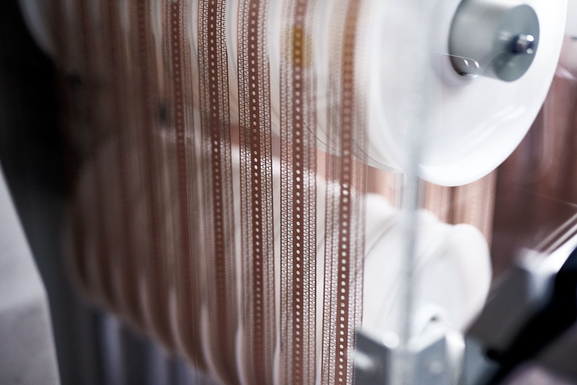
Minimize waste and loss in the wafer dicing process
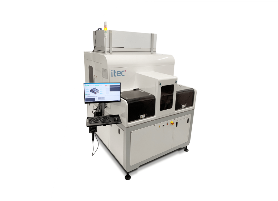
The most cost-efficient diced-wafer inspection system on the market. With a high-speed and high-precision 2D vision scanning system, the PHIXEL WIF guarantees exceptional throughput without compromising inspection quality and accuracy. Moreover, the Advanced Defect Classification (ADC) by hybrid analysis functionality of this inspection system will enhance manufacturing efficiency and competitiveness.
PHIXEL WIF offers inspection after wafer dicing to detect surface defects or inspection after saw singulation of molded package (QFN/DFN) to detect package and marking defects.
Application
- Inspection after wafer dicing to detect surface defects
- Inspection after package singulation to detect package, mark, lead, and plating defects
Key features
- 2D surface inspection, stationary camera
- 128-thread processor
- Supports high-density wafer up to 500K dies
- FOV 25 mm, 1.7 µm pixel resolution or 0.85 µm by upscaled image
- Auto 2D barcode reading
- Hi-end vision performance
- High throughput at high-volume manufacturing rate
- Granit base inspection work holder
- Supports 6", 8", 12" wafer on Frame Film Carrier
- Automatic wafer map match
- Two cassettes at input loader
- SEMI standard with SECS/GEM interface
Imaging system
- Camera: 16K line scan monochrome
- Number of camera(s): 1
- Resolution/Field of view:
1.7 µm, FOV: 25 mm /
3.4 µm, FOV: 50 mm (Optional) - FOV 25 mm with 2 magnifications or selection or 0.85 µm by upscaled image
- Minimum object detection: 2 pixels resolution
- Lighting: Coaxial
Inspection categories
- Program mode: Fast programming for common reject criteria
- Reject treatment: Electronic wafer map
- Inspection view: Top view
Inspection items
- Die related: Chipping. Damaged bump larger than percentage of bump area. Bump diameter. Shorted bumps contact. Missing bump. Scratch. Probe mark size larger than percentage of bump area. Cracked die. Kerf shifting. Discoloration