 中文
中文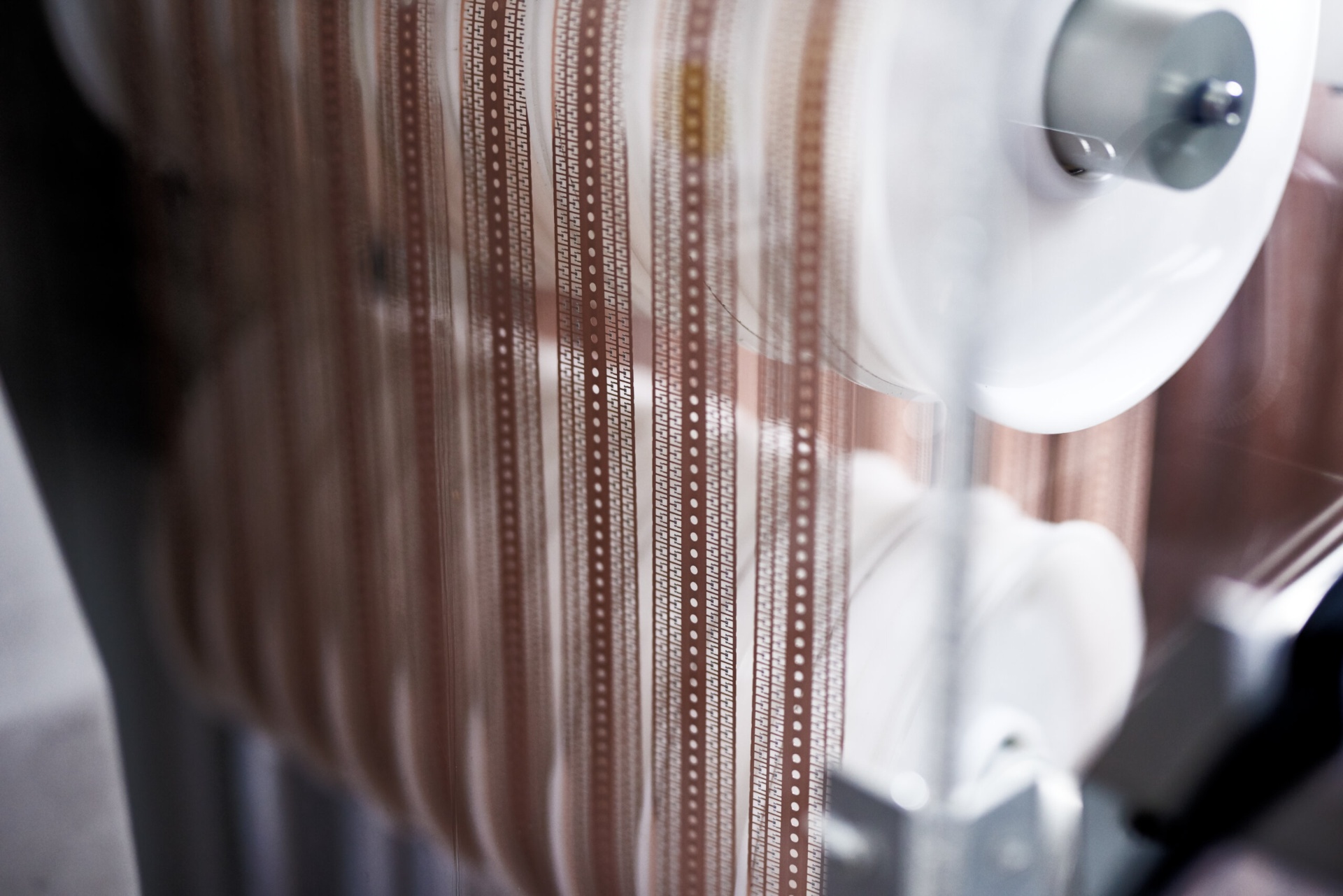
30 years of innovation
ITEC’s first BiM semiconductor equipment line was developed in Hong Kong for Philips in the late 80’s. A few years later, in 1991, it became a standalone department within Philips Semiconductors. Today, ITEC is recognized worldwide for its innovative technologies.
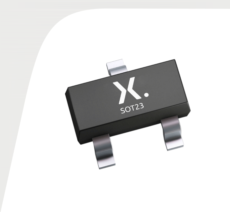
BiM revolutionized manufacture of the outstandingly successful SOT23 package. By coupling die bonding, wire bonding, molding, and plating in one flow line—together with the development of the Parset testing platform—productivity, yield and quality were transformed.But this step change was only the beginning. ITEC’s commitment to offering clients affordable upgrades saw machine speeds increase from 6k units per hour (UPH) all the way up to 72k and beyond.
With Philips’ Hong Kong team working hand-in-hand with colleagues back in Nijmegen, in the Netherlands, a continual flow of new and improved products was developed to support the production and testing of ever smaller and more sophisticated packages.
Best in class, lowest total cost of ownership (tcoo)
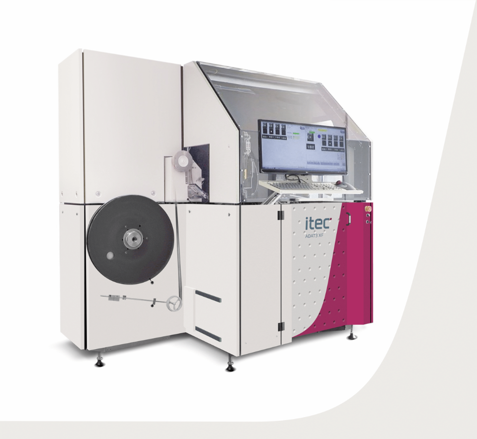
As the new millennium dawned, development continued apace, in both production and testing/inspection. In particular, from the year 2000 onwards the now-famous ADAT3 assembly platform, constantly refreshed and upgraded, continued its leadership in high volume pick and place operation, right up to the present day. Similarly, the Parset family remains the benchmark for analog testing of small signal to power MOS devices, setting the standard for high-speed semiconductor production testers. Built-in versatility and flexibility, and ITEC’s adoption of smart manufacturing/Industry 4.0 techniques such as our ITECore factory automation system, ensure that we continue to achieve our goal of offering best in class semiconductor manufacturing capability. This smart manufacturing approach ensures the highest quality and yields coupled with the lowest total cost of ownership.
ITEC as an independent entity
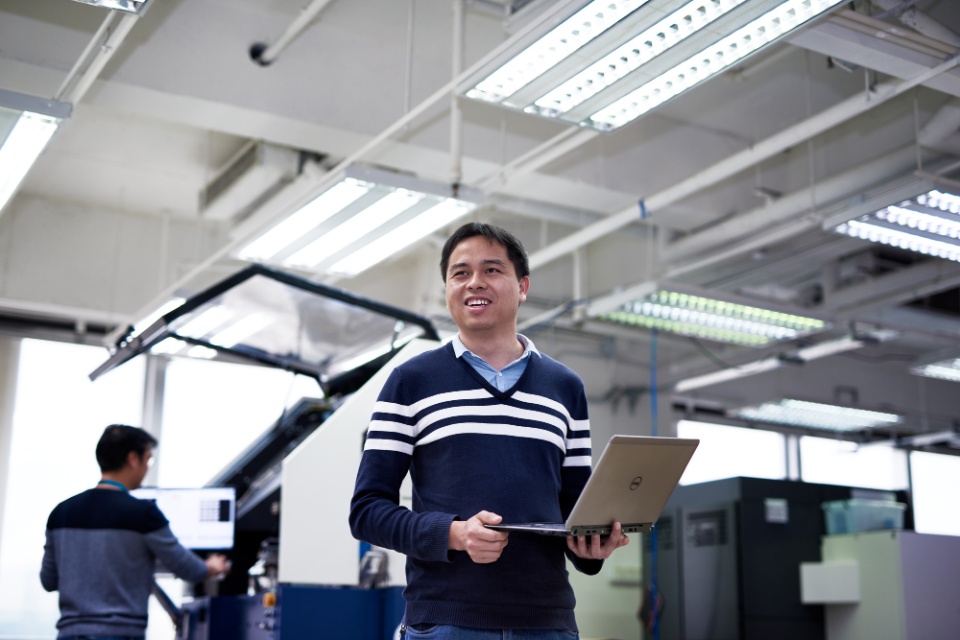
With Phillips Semiconductors becoming NXP in 2006 and NXP Standard Products becoming Nexperia in 2017, ITEC has seen many changes. However, since 2021, as ITEC B.V., we have been an independent entity within the Nexperia Group. We have over 250 employees worldwide, consisting of around 35 nationalities divided more or less equally between Europe and Asia.
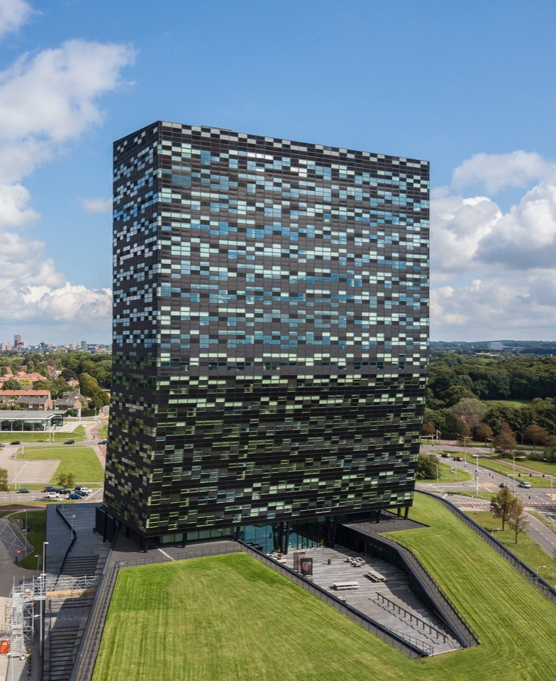
In Hong Kong we work from the innovative Science and Technology Park, where we develop our state-of-the-art Inspection, AI and deep learning solutions. At the company headquarters in the Netherlands, we benefit from Nijmegen’s position as a leading center for advanced mechatronics, process engineering, smart manufacturing, and other high tech innovation capabilities.
High accuracy, high speed, high quality
Today, we work with leading semiconductor manufacturing companies who are looking for a competitive technological edge. Currently we have an installed base of over 2,500 test and assembly systems, with over 3,700 different tools connected to the ITECore factory automation system. Our latest generation ADAT3 XF realizes a (record-breaking) output of 1.2 million devices per day, so our installed base enables production of over 100 billion semiconductors a year – compared with around 4.5 billion in 1991!
As a reliable partner we bring more than just breakthrough technologies to our customers; we back that up with over thirty years of process expertise and experience. Our tailored solutions enable our clients to strengthen their market positions by excelling in accuracy, speed and quality, while seeing significant gains in productivity and sustainability, at the lowest total cost of ownership.