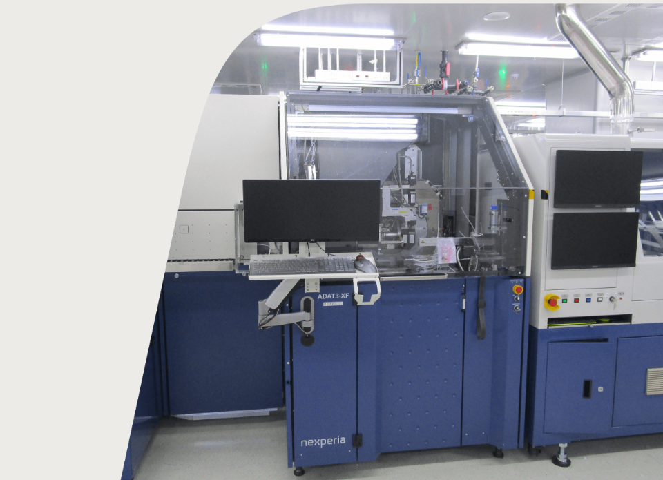
A breakthrough in cost, quality, and productivity
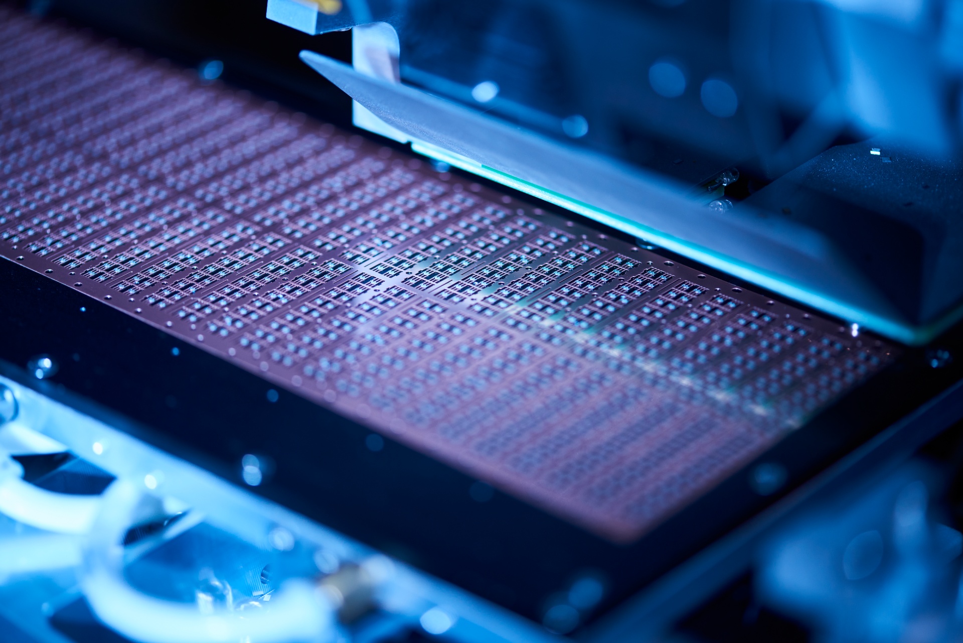
The only product in the market offering an in-line strip-to-strip die bonder solution. The ADAT3 XF DBS receives strips directly from one machine, processes them, and feeds them to the next — maximizing your productivity. Handling ultra-small and medium die at unparalleled speed, it easily connects to top and bottom screen-print equipment. This die bonder is also equipped with automated wafer change and high-definition optics for on-the-fly quality inspection.
Performance
Up to 60.000 units per hour
Supports 8 to 12 inches wafer on frame film carrier
Strip size
100 x 300 mm
Solder paste/Glue
Die size
Minimal: 0.2 x 0.2 mm
Maximum: 7 x 9 mm
High throughput at high-volume manufacturing rate
Belt in, belt out
Full die traceability (strip E142 – wafer)
Auto recipe download: Manufacturing Execution System (MES) interface
SECS/GEM interface with E142
Solder paste power application, SO8, DPAK, and SOD123/128 SOT669
Speed
Up to 60.000 units per hour (depending on die size, lead frame pitch, glue/solder type and selected quality inspections)
Die Range
Length, width: 0.2 x 0.2 mm to 7 x 9 mm
Aspect Ratio: 1:1 - 1:3
Thickness: 50 - 400 µm
Lead frame size
Minimum length, width: 100 x 40 mm
Maximum length, width: 300 x 100 mm
Thickness: 0.1 - 1.0 mm
System accuracy
Small die (≤ 1 mm): XY: 1 σ xy ≤ 5 μm. Rotation: 1 σ φ ≤ 1˚
Large die (≥ 1 mm): XY: 1 σ xy ≤ 5 μm. Rotation: 1 σ φ ≤ 0.3˚
Pick and place force: 0.2-1.5 ± 0.1 N
Wafer handling
Wafer size: 6 - 12 inches
Wafer frame: 8 - 12 inches
Steel/Plastic Film Frame Carrier (FFC)
Foil Tension: Programmable expander (8 inches: 1 - 10 mm, 12 inches: 1 - 15 mm)
Automatic wafer change and expander
Automatic barcode reader
Lead frame handling:
Conveyor belt loading and unloading according SMEMA protocol
Pick up tooling
Vespel collet
Rubber tip
Four-sided collet
Push-up needle
Imaging system
Number of cameras: 4
Resolution/Filed of View (FOV) glue: 0.3 MP camera (3.2 UM/pixel), FOV 2.1 x 1.4 mm
Resolution/ Filed of View (FOV) pick-up and backside: 5.0 MP camera (2.3 UM/pixel), FOV 5.6 x 4.7 mm
Resolution/ Filed of View (FOV) post-bond: 5.0MP camera (4.6 UM/pixel), FOV 11.3 x 9.4 mm
Resolution/ Filed of View (FOV) sidewall: optional
Minimal object detection: 10 micrometres (μm)
Lighting: coaxial and ring light, including multicolor light
Inspection categories
Program mode: Fast programming for common reject criteria
Reject treatment: Strip map (E142) and reject bin
Inspection view: 4 cameras, (1) glue, (2) pre pick
(3) back, (4) post-bond
Inspection items
Die-related: Top chipping, backside chipping. Damaged. Die size/die ratio. Scratch. Cracked die. Discoloration
Glue-related: Drop size. Drop shape
Post-bond related: Die alignment (position, size, rotation). Glue fillet
Automation:
Wafer map SEMI E142 format, SECS-GEM mpa exchange
Start and reference die functionality
Automatic Product Replacement
MES Interface including auto recipe download
Monitoring of critical process parameters during production. Automatic stop function when parameter out of control
Servo, bond-force and vacuum auto-diagnostics functionality to check health status of the machine
Machine dimensions
Length, width, height: 2200 x 2100 x 1250 mm3
Net weight: 1950 kg

 中文
中文