 中文
中文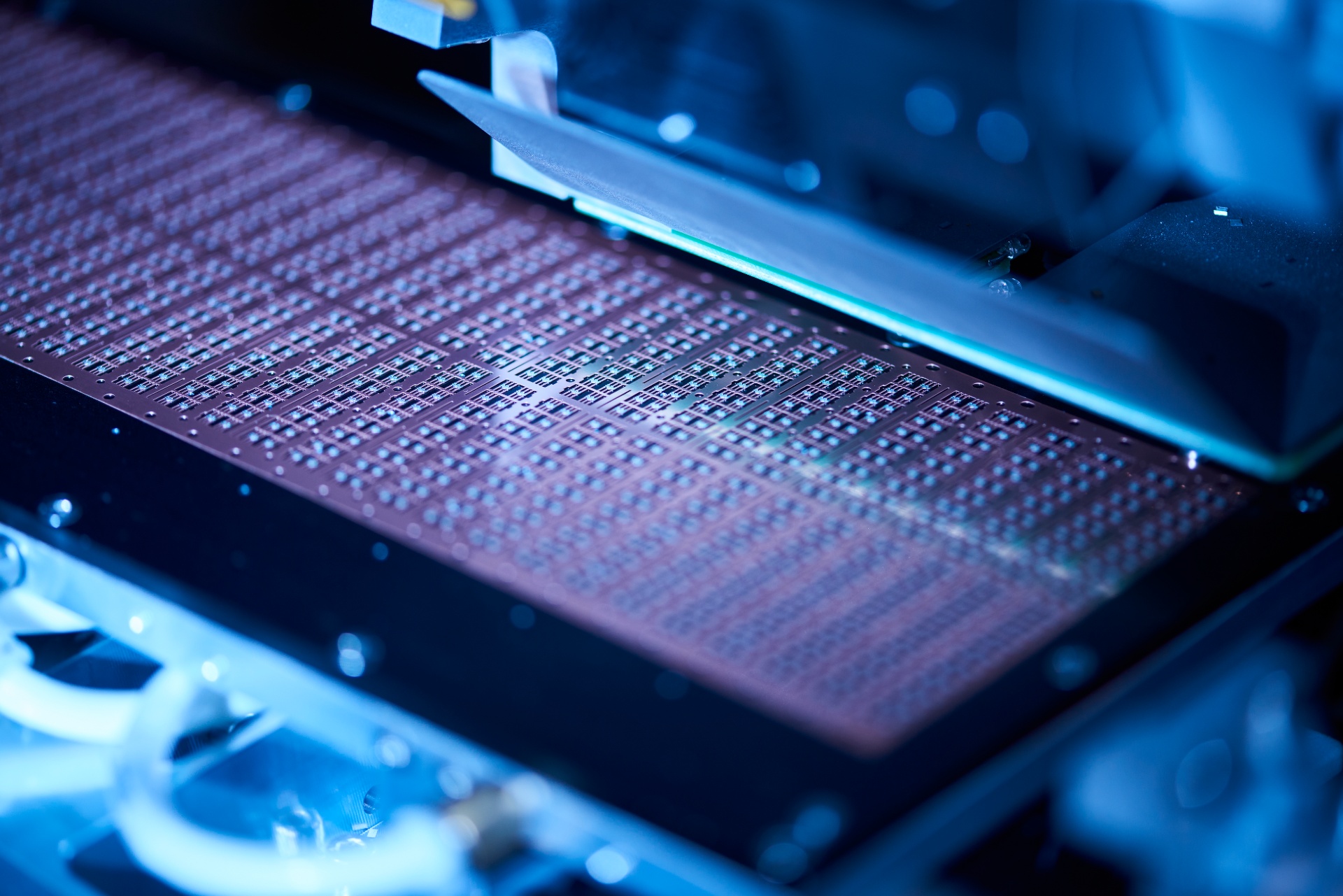
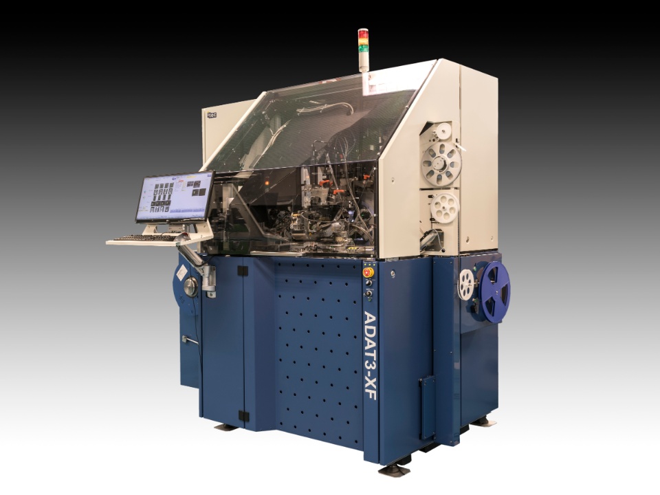
Up to 60.000 units per hour
Gain maximum productivity at the lowest costs. At 20% faster than anything in the market, this is the die sorter for wafer-level CSP/micro CSP applications. It handles the smallest die with automatic wafer change. The ADAT3 XF DS also inspects all six sides of the die without any speed penalty, securing quality in this critical last process step — without compromising productivity or cost.
Performance
Up to 60.000 units per hour
Supports 8 to 12 inches wafer on frame film carrier
Tape width
8 - 12 mm
Sidewall inspection
Die size
Minimal: 0.2 x 0.4 mm
Maximal: 5 x 5 mm
High throughput at high-volume manufacturing rate
APR auto-product replace
In-tape inspection
Automatic reel changer: optional
Full die traceability: tape – wafer
Auto recipe download (MES interface)
SECS/GEM interface with E142
Speed
Up to 60.000 units per hour flip or non-flip
Die Range
Length, width: 0.4 x 0.2 mm to 5 x 5 mm
Aspect Ratio: 1:1 - 1:3
Thickness: 50 - 400 um
Tape handling:
Width: 8 - 12 mm
Pitch: 2 - 8 mm
Thickness: 0.18 - 0.5 mm
Tape specification: embossed carrier tape with pocket hole, punch tape, paper tape, surf tape
Hot sealing: maximum temp 200 °C, maximum force 10 - 80 Newton (N)
Auto reel change, auto tape cutter
System accuracy
Small die (≤ 1 mm): XY: 1 σ xy ≤ 5 μm. Rotation: 1 σ φ ≤ 1˚
Large die (> 1 mm): XY: 1 σ xy ≤ 5 μm. Rotation: 1 σ φ ≤ 0.3˚
Wafer handling
Wafer size: 6 - 12 inches
Wafer frame: 8 - 12 inches
Steel/Plastic Film Frame Carrier (FFC)
Foil Tension: programmable expander (8 inches: 1 - 10 mm, 12 inches: 1 - 15 mm)
Automatic wafer change and expander
Automatic barcode reader
Imaging system
Number of cameras: 5
Resolution/Field of View (FOV) pick-up and backside: 5.0 MP camera (2.3 UM/pixel), FOV 5.6 x 4.7 mm
Resolution/ Field of View (FOV) post-bond: 5.0MP camera (4.6 UM/pixel), FOV 11.3 x 9.4 mm
Resolution/ Field of View (FOV) sidewall: 12.3MP camera (2.3 UM/pixel), FOV 9.4 x 6.9 mm
Resolution/ Field of View (FOV) Die ON FLIP: 5.0 MP camera (2.3 UM/pixel), FOV 5.6 x 4.7 mm
Resolution/ Field of View (FOV) post-seal inspection: 1.3 MP (3.7 UM/pixel) FOV 9.7 mm
Post-seal inspection: seal-line , index hole, empty, tilted, body outline, product code, marking, chipping
Minimal object detection: 10 micrometres (μm)
Lighting: red ring, coaxial, and back panel light
Inspection categories
Program mode: Fast programming for common reject criteria
Reject treatment: Strip-tape map (E142) and reject bin
Inspection view: 5 cameras, (1) pre-pick, (2) back and sidewall, (3) front/bump, (4) post-bond, (5) post-seal
Inspection items
Die top-related: Top chipping, backside chipping
Damaged. Die size/die ratio. Scratch. Cracked die
Discoloration. Bump inspections (size/connected/missing)
Backside related: Die alignment (position, size, and rotation). Backside chipping
Surface inspection: Punch through inspection. Laser mark inspection. Pin A1
Automation:
Wafer map SEMI E142 format, SECS-GEM mpa exchange
Start and reference die functionality
Automatic product replacement
MES Interface including auto recipe download
Monitoring of critical process parameters during production
Automatic stop function when parameter out of control
Servo, bond-force and vacuum auto-diagnostics functionality to check health status of the machine
Machine dimensions
Length, width, height: 2200 x 2100 x 1250 mm3
Net weight: 1850 kg